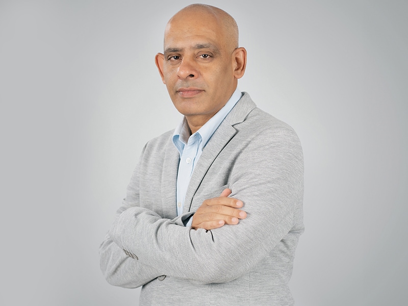
 Raghu Panicker, CEO of Kaynes Semicon
On Friday, Karnataka-based electronic system design and manufacturing solutions supplier Kaynes Technology inaugurated its ninth facility in Telangana’s Hyderabad. About 40 kilometres away from the main city, the plant is located at the industrial park in Kongara Kalan in Ranga Reddy district, close to the upcoming Foxconn factory. The advanced electronics unit will primarily produce smart meters, with the gradual allocation of lines to outsourced semiconductor assembly and testing (OSAT).
Last year, in October, the 35-year-old company formed Kaynes Semicon and announced setting up OSAT in Telangana under the Central government’s Rs76,000 crore semiconductor incentive scheme. Kaynes is still waiting for a sign-off from the government, which has reportedly suggested it set up the unit in Gujarat’s Sanand district instead. At the same location, American chip giant Micron and Murugappa Group’s CG Power are also putting up chip assembly, testing, marking, and packaging (ATMP) units. The newly inaugurated facility was earlier dedicated only to OSAT manufacturing, which will now focus on electronics manufacturing services.
Kaynes Semicon already has three customers from Singapore, Taiwan, and the Philippines on board. It’s waiting for approval to come in to start the construction and manufacturing. On the sidelines of the event, Forbes India caught up with Raghu Panicker, CEO of Kaynes Semicon, who shared more details on why they decided to foray into OSAT, their global technology partners, the delay in getting approval from the government, and more. Edited excerpts:
Q. When are you expecting to receive approval from the central government for the OSAT project? Why is it delayed?
We are almost a week to 10 days away, and the approval should be in. This is a part of their 100-day program after the government comes into being. There were other priority sector projects, so semiconductors are yet to be looked at. I’m sure in the coming days, you will hear some good news on our project as well as a few other projects.
Q. There’s confusion with picking the factory location. It was supposed to be Telangana earlier, and now reportedly it is Gujarat. What will be the final destination?
I have no comments on that because I still don’t have the approval. Yes, we did buy land in Gujarat, but it’s part of our expansion plans. So our application started with Telangana for OSAT. We got the land, and you can see we put in a facility for EMS. Land is a requirement. We have a large backlog of orders. We clocked Rs1,900 crore of revenue last year, and we are looking to do over Rs3,000 crore this year, which means that we need infrastructure to grow.
Q. Why did Kaynes Semicon specifically decide to foray into OSAT?
Kaynes’ electronics manufacturing services (EMS) business is uniquely placed. We are into manufacturing printed circuit board assemblies (PCBAs). There are two components that come in: The semiconductor component and the bare board. These two components are imported at this point in time. So it is necessary that we start some local manufacturing. We ourselves will consume these semiconductor packages and PCBs because we are an EMS player. Hence, we are building two plants. From backward integration, we are putting a Kaynes semiconductor plant under Kaynes Semicon, which is OSAT. We have another subsidiary called Kaynes Circuits, and we are putting up a bare-board PCB plant. We are trying to reduce the import, and plus, it’s self-consumption for us. This aligns with our thought process as far as semiconductor manufacturing is concerned. The idea is to reduce the price of the end product. We are a large supplier of PCB modules for automotive. If you look at the power devices that go inside the module and if I am able to manufacture them, we’re trying to reduce the price.
Everything put together, we’ve announced an investment of Rs6,500 crore, out of which Rs5,000 crore is for OSAT and the rest for bare-board PCB.
Q. Will this OSAT be doing traditional packing or advanced packing?
About 70 percent of our OSAT will be doing advanced packaging, and that’s the difference we are going to bring to India. There’ll be 30–35 percent of traditional packaging. But we are starting with substrates for co-packaged optics. The MOU we signed with Singapore-based fabless system development company Light Speed Photonics is a very advanced technology. In the next six to eight months, I will have my first line with them done, and my first package will be rolled out in the next six to eight months. I’m just waiting for approval.
Q. Who are your global technology partners?
We have three technology partners for semiconductor packing: Globetronics from Malaysia, Aptos Technologies from Taiwan, and AOI in Japan. We have also invested in California-based Mixx Technologies.
Q. Is India tapping into the right part of the semiconductor supply chain?
In the last 30 years, we’ve mastered the art of design, and that’s the high-value chain. Now, beyond that, what do we do? It’s manufacturing, and that’s a capital-intensive and labour-intensive activity. India, as a country, needs all that. Slowly, this will be self-consuming. There’s one fab that was announced by Tata. There are a few more in line. The entire value chain is in the making.
