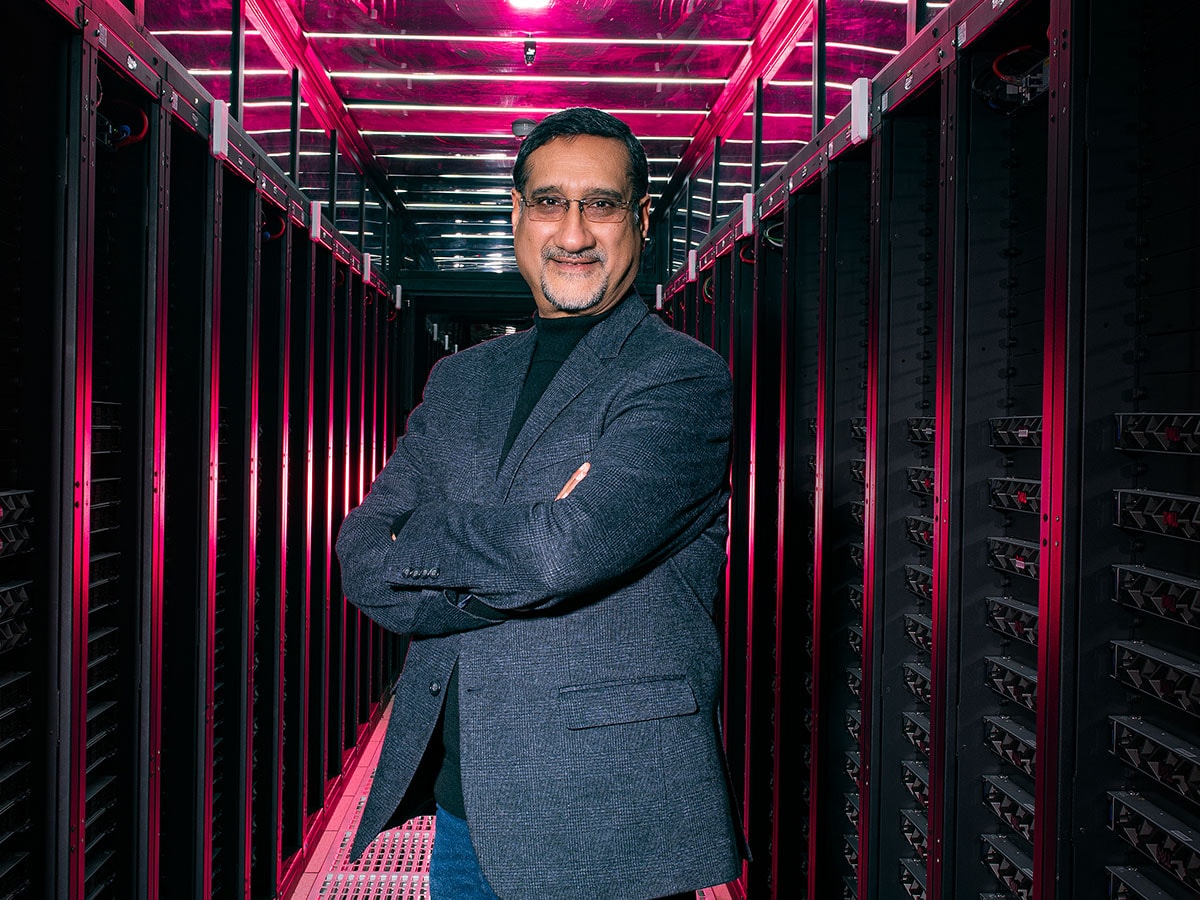
Jaswinder Ahuja, Corporate Vice President, International HQ and India Managing Director, Cadence Design Systems
Image: Amit Verma
Jaswinder Ahuja still remembers the one-line mandate he was given when he was elevated to managing director in India at Cadence Design Systems in 1996.
“I don’t want any part of my organisation to be a second-class citizen,” he recalls as the brief from the company’s then-global head of R&D Shane Robinson. “And he left it to me to interpret what that meant and how we went about building the India operations,” Ahuja, who’s also corporate vice president, international HQ, at the EDA company, tells Forbes India.
EDA stands for electronic design automation, the technologies for which Cadence is best known. These are the software and hardware tools used in the design of integrated circuits (ICs), systems on chips (SoCs), and electronic systems. “The EDA domain or the domain that we work in is all about helping our customers deal with ever-increasing complexity of design,” Ahuja says.
Ahuja was engineer number five in 1987 at Gateway Design Automation, the company that developed Verilog, the hardware description software that chipmakers such as AMD, Nvidia, Qualcomm or Texas Instruments use to this day. When Cadence acquired GDA in 1989, Ahuja became part of its small India team.
 Today, Cadence has over 4,200 employees in India across five locations. That represents one third of the company’s total headcount and close to 40 percent of its R&D resources, he says. Because we are heavy on engineering and light on the corporate functions in India.
Semiconductor experts such as Ahuja know that some features are critical, and they need to be burnt into a physical chip but others can be offered via software. This makes all the difference because if a feature etched into a wafer doesn’t function as envisioned, fixing it can be costly and time consuming. Software on the other hand, can be coded differently and quickly.
And with AI (artificial intelligence) in the mix, software is perhaps an even more attractive option. This is where India’s “fabless design” semiconductor engineers—most of them are already at in-house centres such as those of Cadence or AMD—have a big opportunity.
“Over the last couple of years, one of the areas where our teams have been deeply engaged in and have made significant contributions in is in incorporating AI techniques and AI algorithms into our software,” Ahuja says.
Also read: We run the digital backbone for 100,000 BT Group employees: Jay Doshi
When one looks at the rate at which the complexity of semiconductor design is increasing and the capability that the designers have, there is “productivity gap”. And it’s not possible for companies to ramp up their teams easily to bridge that gap. Therefore, customers expect the algorithmic enhancements in Cadence’s EDA software to make a difference.
Companies such as Cadence, building highly complex products, rarely have any one site taking complete ownership of any given product, he points out. That said, the teams in India are playing an indispensable role in developing Cadence’s AI software, Ahuja says. For example, they are involved in a lot of the experimentation and simulations to figure out which algorithms might work as intended to deliver the required outcomes.
Cadence India is also helping to develop what are called semiconductor IP (different from intellectual property), which are building blocks of design for components or parts of components such as interfaces for, say, a USB connector and so on. As new memory interfaces are being developed to support AI computation, Candence India is in the thick of it.
“With new standards coming up, especially in the memory interfaces space, a lot of that IP is being driven out of India,” Ahuja says.

Overall, today it’s still the headquarters that usually decides on the ‘what, why and when’ of a product, meaning what to develop, why and when to release it—the upstream strategy. The who and the how is increasingly coming down to sites such as the India GCC, he says.
The aspiration is that in the future the India team should play a bigger role in setting more of the business strategy as well.
“We are on a journey where we are maturing,” Ahuja says, referring not only to Cadence India but also the semiconductor ecosystem in India. “If you fast forward to five, maybe 10 years, we should be in a position where we would be making many of those decisions right here in India, in leading and driving product portfolios.”
“We are not there today, but that’s both the aspiration and the opportunity,” he adds.
(This story appears in the 21 February, 2025 issue
of Forbes India. To visit our Archives, click here.)